
Course Title: Digital Logic (3 Cr.)
Course Code: CACS1O5
Year/Semester: I/I
Class Load: 5 Hrs. / Week (Theory: 3 Hrs, Practical: 2 Hrs.)
Course Description
This course presents an introduction to Digital logic techniques and its practical application in computer and digital system.
Course Objectives
The course has the following specific objectives:
– To perform conversion among different number systems
– To simplify logic functions
– To design combinational and sequential logic circuit
– To understand industrial application of logic system.
– To understand Digital IC analysis and its application
– Designing of programmable memory
Course Contents
Unit 1 Introduction [2 Hrs.]
1.1 Digital Signals and Wave Forms
1.2 Digital Logic and Operation
1.3 Digital Computer and Integrated Circuits (IC)
1.4 Clock Wave Form
Unit 2 Number Systems [5 Hrs.]
2.1 Binary, Octal, & Hexadecimal Number Systems and Their Conversions
2.1.1 Representation of Signed Numbers-Floating Point Number
2.1.2 Binary Arithmetic
2.2 Representation-of BCD-ASCII-Excess 3 -Gray Code —Error Detecting and Correcting Codes.
Unit 3 Combinational Logic Design [16 Hrs.]
3.1 Basic Logic Gates NOT, OR and AND
3.2 Universal Logic Gates NOR and NAND
3.3 EX-OR and EX-NOR Gates3.4 Boolean Algebra:
3.3.1 Postulates & Theorems
3.3.2 Canonical Forms – Simplification of Logic Functions
3.5 Simplification of Logic Functions Using Karnaugh Map.
3.5.1 Analysis of SOP And POS Expression
3.6 Implementation of Combinational Logic Functions
3.6.1 Encoders & Decoders
3.6.2 Half Adder, & Full Adder
3.7 Implementation of Data Processing Circuits
3.7.1 Multiplexers and De-Multiplexers
3.7.2 Parallel Adder -Binary Adder-Parity Generator /Checker-Implementation of Logical Functions Using Multiplexers.
3.8 Basic Concepts of Programmable Logic
3.8.1 PROM
3.8.2 EPROM
3.8.3 PAL
3.8.4 PLA
Unit 4 Counters & Registers [16 Hrs.]
4.1 RS, JK, JK Master – Slave. D & T Flip flops
4.1.1 Level Triggering and Edge Triggering
4.1.2 Excitation Tables
4.2 Asynchronous and Synchronous Counters
4.2.1 Ripple Counter: Circuit and State Diagram and Timing Waveforms
4.2.2 Ring Counter: Circuit and State Diagram and Timing Waveforms
4.2.3 Modulus 10 Counter: Circuit and State Diagram and Timing Waveforms
4.2.4 Modulus Counters (5, 7, 11) and Design Principle, Circuit and State Diagram
4.2.5 Synchronous Design of Above Counters, Circuit Diagrams and State Diagrams
4.3 Application of Counters
4.3.1 Digital Watch
4.3.2 Frequency Counter
4.4 Registers
4.4.1 Serial in Parallel out Register
4.4.2 Serial in Serial out Register
4.4.3 Parallel in Serial out Register
4.4.4 Parallel in Parallel out Register
4.4.5 Right Shift, Left Shift Register
Unit 5 Sequential Logic Design [6 Hrs.]
5.1 Basic Models of Sequential Machines
– Concept of State
-State Diagram
5.2 State Reduction through Partitioning and Implementation of Synchronous Sequential Circuits
5.3 Use of Flip-Flops in Realizing the Models
5.4 Counter Design
Laboratory Works
- Gates using Active and Passive Elements
- Half Adder and Full Adder
- 16:1 Multiplexer
- 1:16 Demultiplexer
- Digital Watch by Counters
- Shift Resistors
Teaching Methods
The general teaching methods includes class lectures, group discussions, case studies, guest lectures, research work, project work, assignments (theoretical and practical), and exams, depending upon the nature of the topics. The teaching faculty will determine the choice of teaching pedagogy as per the need of the topics.
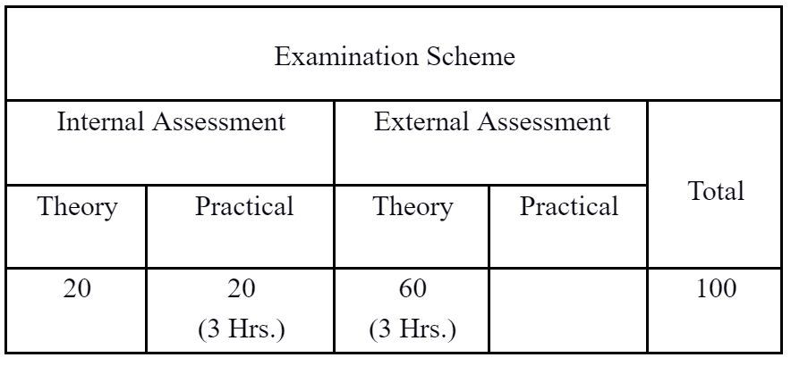
Evaluation

Text Books
- Floyd, “Digital Fundamentals”, PHI.
- Morris Mano. “Digital Design”, Prentice Hall of India.
- Tocci.R.J, “Digital systems-Principles & Applications”-Prentice Hall of India.
Reference Books
- B. R. Gupta and V.Singhal, “Digital Electronics” 4th Edition, S.K Kataria & sons, India.
- Flctcher.W.I., “An Engineering lrproach to Digital Design”, Prentice Hall of India.
- Millman & Halkias ,”Integrated ElectrOnics”.
- V.K.PUR1, “Digital Electronics”, TMH.,
To download full Syllabus CLICK HERE